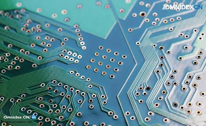
PCB (Printed Circuit Board) manufacturing is a time-consuming and complicated process. PCBs are the foundation component of electronic assemblies. It is therefore imperative PCBs are produced to the highest possible standard.
The most common PCB types are rigid (hardboard), flexible (copper and cover-lay), and rigid-flex (integrated hardboard and flex circuits). In this article, we will discuss the processes used to manufacture rigid PCBs, which come in three varieties: single-sided, double-sided, and multilayer.
PCBs can be manufactured using various materials. Most rigid PCBs are made using glass fibre, a material known as FR-4. Besides FR-4, other materials such as phenolic paper can be used for low-cost commercial products. High performance, high-frequency designs often use Teflon or PTFE. Flexible, rigid-flex designs typically use polyimide.
The PCB manufacturing process can be summarised by the following 13 steps:
CAD operators must design/layout the PCB before the manufacturing process can begin. Guided by the schematic of the working circuit, they aim to optimise space, and reduce track length and materials whilst ensuring that tracks are of sufficient size for the rated current.
Following the completion of the design, the PCB manufacturer receives a set of documents exactly specifying the build. Gerber files in the document include information on layers, drill files, pick and place data, and text notes.
The fabrication prints provide all PCB specifications, dimensions, and tolerances, as well as fabrication notes that are crucial to the build.
PCB houses begin creating manufacturing process plans and artwork packages once they receive the designer’s documentation. The fabrication specification describes substrate material type, surface finish, plating, panel arrays, and routing of processes to determine the plan.
Additionally, a film plotter is used to create physical copies of artwork. Artwork for the PCB will include solder mask and nomenclature markings as well as artwork for all layers of the PCB.
As part of the material preparation process, the designer specifies the type of material, core thickness, and copper weight. With rigid PCBs that are single-sided or double-sided, no inner-layer processing is necessary prior to drilling. Similarly, if the PCB has more than one layer, material preparation is also undertaken for the inner layers, which are typically much thinner cores to be assembled to a predetermined thickness.
Typically, production panels are 18″x24″, although any size can be used if within the manufacturer’s capabilities.
Following preparation of the inner layers for their size, material type, core thickness, and copper weight, the layers are sent for drilling of the tooling holes before being printed. Each layer is then coated with a photoresist on both sides before being printed.
By aligning the inner-layer artwork and tooling holes, each side is then exposed to UV light, allowing the optically negative pattern of trace and feature identification to be seen. UV light breaks down the chemical in the photoresist, while a developing bath is used to remove the unexposed chemical.
An etching process is then used to remove the copper exposed. Under the photoresist layer, copper tracks are thus left behind. Etching is a process where the concentration of the etchant and the time of exposure both play an important role. After the resist is stripped off, the inner layers are left with traces and features.
Automated optical inspection systems are typically used to inspect PCB layers, followed by post-etch punches to optimize the holes for lamination tooling.
As an example, a four-layer board stack up might look like this:
CNC controlled multistation drill machines and carbide drill bits specifically designed for drilling PCBs are used for the drilling process. A typical via hole is drilled at over 100K RPM with a diameter of .006″ to .008“.
Through the drilling process, a smooth, clean hole wall is created, and the drilled hole is used for connectivity within the layer after plating, and non-via holes will eventually house thru-hole components.
Drilling of non-plated holes is usually a secondary operation.
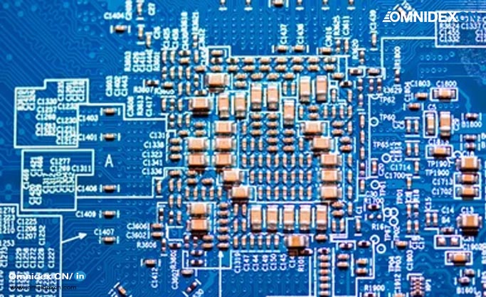
Electroplating is widely used when plated through- holes are needed in PCB production. During electro-plating, copper is deposited onto a conductive substrate via chemical treatment methods, and the copper thickness is increased via subsequent electro-plating methods to a specific thickness of the design, usually 1 mil or more.
Processes for processing the outer layer are nearly identical to those for processing the inner layers. Photoresist is coated on both sides of the top and bottom layers. As each side is aligned with the outer-layer artwork and the holes in the tooling, it is then exposed to UV light, which reveals the linear optically negative pattern of traces and features.
By exposing the photoresist to ultraviolet light, the chemical is attracted to the copper surface, and the remainder is removed in a developing bath. Using an etching process, the exposed copper will be removed.
Copper traces are left behind under the photoresist layer. The outer layers are left with traces and features, leftover from removing the resist. With Automated Optical Inspect, outer-layer defects can be found before the solder mask is applied.
Solder masks are applied similarly to inner and outer layers. Instead of a photoresist, the entire surface of the production panel is covered with a photo-imageable mask.
In this way, both the top and bottom layers can be shot. Once the top and bottom layers are exposed, the mask is removed in the imaged areas. Exposing only the areas that will be soldered, it allows components to be placed and assembled. It also limits the finish of the PCB to the exposed areas.
The final surface finish can be chosen from a few options. The most common solder types are gold, silver, OSP, lead-free solder, and leaded solder. However, the most appropriate type depends on the design. Electroplating is used to apply gold and silver, while hot air soldering is used to apply lead-free and lead solder.
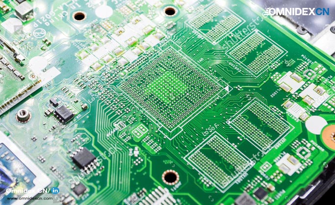
The surface of most PCBs has screen-on markings. There are markings for various assembly processes, including polarity markings and reference designators. Some markings can be as simple as identifying the part number or the manufacturing date.
In most cases, PCBs are made in a full production panel and must be cut to their manufacturing profiles. The PCBs are typically arranged in arrays to facilitate assembly and there are too many array types to describe.
The majority of arrays are profiled on a CNC router using carbide cutters or scored using diamond coated saw-like cutters. Typically, the assembly team, which typically approves the array set up in the early stages, determines which method is appropriate. The two methods are equally effective.
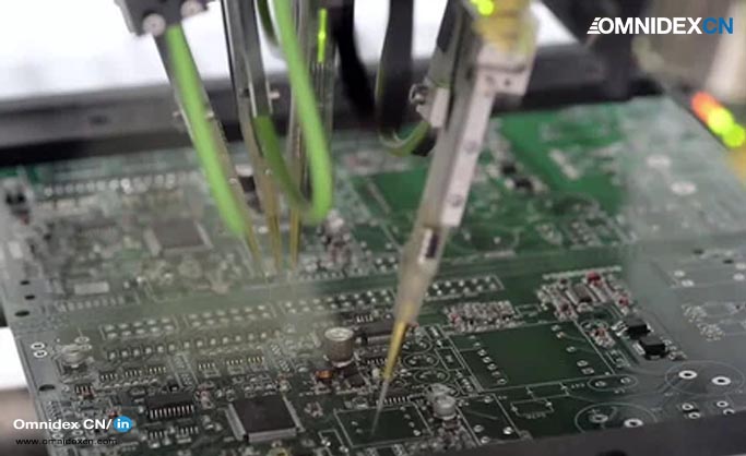
PCB manufacturers generally test their circuit boards using flying probes or beds of nails. Depending on the product volume and the equipment available, different testing methods are used. The netlist files are part of the original Gerber data and are used to create a test program. A PCB house will be able to check for circuit shorts and open circuits with this data.
With over 480+ years of combined experience, we are more than confident in providing electronic/electrical components to meet all your needs. Every product is subject to a rigorous QC process to ensure high performance and reliability, with a straightforward money-back guarantee!
Whether you are an emerging start-up company or a blue-chip corporation, we are keen on providing the most adequate solution for your next project. Contact Us to discuss more details or learn more about our other manufacturing processes and services.
Contact our Customer Service and let us know how we can help to catapult your next project to success.

If you are looking for metal casting services, our brochure is a great way to discover what Omnidex has to offer. You can download HERE or EXPLORE HERE to learn more or .

If you are looking for metal casting services, our brochure is a great way to discover what Omnidex has to offer. You can download HERE to learn more.
Copyright © 2024 Omnidex. All rights reserved.